Research Interests:
Synthesis and characterization of novel nanomaterials including semiconducting nanowires, nanotubes, metal oxide nanowires and nanodots;
Study on electronic transport, optical and mechanical properties of low dimensional nanomaterials and nanocomposites;
Applications of nanomaterials in structural and functional composites and in energy storage;
Application of nanoscience to biology and medicine;
Fabrication and test of nanoelectronic devices.
Research highlights:
·
Dye Sensitized Solar Cells
The research is to develop high efficiency dye sensitized solar cell through innovating its photoanode and counter electrodes. In this project, exploiting the unique anisotropic photocatalysis of rutile crystal, we expect to develop a multiple step growth approach via the assistance of self-assembled monolayer (SAM) to synthesize long rutile nanorod arrays with controllable structure for high efficiency DSSCs. Besides titanium dioxide nanorods, carbon nanotube thin film and its composite with TiO2 will be used to fabricate novel photoanode and counter electrodes for high efficiency solar cells at low cost. Through this research, we aim to understand the electron transport mechanism in the CNT integrated photoanode and counter electrode and to improve the solar cell efficiency by optimizing the solar cell structure at the nanoscale.
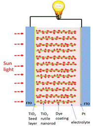
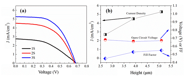
Figure caption. Schematics of TiO2 nanorod dye sensitized solar Cell. (a) J-V curve of the DSSCs made from the 1S,
2S and 3S NR sample. (b) The fill factor
(FF), short circuit current (Jsc) and open
circuit voltage (Voc)) as a function of
the nanorod height.
·
Nanostructured
thermoelectric materials for power generation
Thermoelectric (TE) materials can
be used to develop solid-state power generator based on the Seebeck effect and solid-state refrigerator based on the Peltier effect. The TE material based energy conversion devices will help to solve the
energy crisis because they can harvest waste thermal energy and then convert it
to electrical energy (see Figure
below). The objectives of this research are to (1) develop adequate and
efficient hydrothermal and solvothermal techniques to synthesize nanostructured
TE materials such as bismuth selenide (Bi2Se3), skutterudite (CoSb3), lead telluride
(PbTe), and indium doped lead telluride (InxPb1-xTe), and (2) understand how the quantum-confinement
effect and the interface scattering to phonons affect the thermoelectric
properties of the materials.
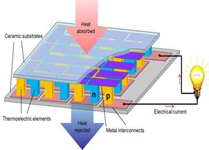
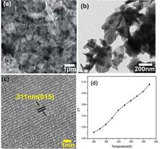
Figure. Left: Schematic of a thermoelectric generator. Right panel: SEM and TEM images of the as–prepared Bi2Se3 samples synthesized in DMF at 200ºC for 24 h. a) SEM image, b) TEM image, c) HRTEM image, d) Figure of merit (ZT) vs.
temperature. For details, please refer to Kadel et al., “Synthesis and Thermoelectric Properties of Bi2Se3 Nanostructures” Nanoscale Research Letters 6:57, 2011.
·
Electron filed emission
properties of carbon nanotube arrays synthesized by plasma enhanced chemical
vapor deposition
Carbon nanotubes (CNTs) have been considered as the next generation field emission material due to their large aspect ratio, high mechanical stiffness, good electrical conductivity, and excellent thermal and chemical stability. Vertically aligned multi-walled carbon nanotubes (MWCNTs) were grown on Cu substrates by PECVD and were then treated by NH3 plasma to modify their microstructure. A great improvement on the field emission properties of the MWCNTs was obtained after the plasma treatment. Specifically, the MWCNTs after 1.0 min plasma treatment demonstrated the best field emission performance with the field enhancement factor increasing from 319 to 546, the turn-on electric field decreasing from 11.93 V/mm to 8.84 V/mm, and the highest emission current reaching 0.85 mA, as compared to the untreated sample. The improvement was attributed to the morphology change: the tapered structure of the MWCNTs generated by the plasma etching and the increased inter-tip distance due to the cluster structure of the thin tips. The open-ended tips and the increased structural defects introduced by NH3 plasma also played a role in the enhancement of field emission properties of the MWCNTs.
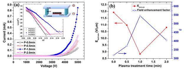
Figure. Field emission characteristics of the MWCNTs before
and after NH3 plasma treatment. (a) I-V curves. The inset shows the corresponding
F-N plots and the upper
right inset
shows the schematic of
the field emission measurement setup. (b) Field enhancement factor (b) and turn-on
electric field (Eturn-on) of MWCNTs according to NH3 plasma treatment time. For details, please refer to
Chen et al, “Electron field emission properties of vertically aligned carbon
nanotube point emitters” Diamond and Related Materials 25, 134 (2012); Neupane
et al., “Synthesis and field emission properties of vertically aligned carbon
nanotube arrays on copper”, Carbon 50, 2641 (2012),
·
Study
of Radial Modulus of Single-walled Carbon Nanotubes by Atomic Force Microscopy
The understanding of the mechanical properties, especially the radial modulus (radial elasticity), of single-walled carbon nanotubes (SWCNT) is very important in developing SWCNT-based nanodevices. We have measured the radial modulus by combining tapping mode and contact mode atomic force microscopies on as-grown horizontally aligned SWCNTs. It is found that the radius of the SWCNTs has a significant influence on the radial modulus. As shown in the Figure, the measured radial modulus (Eradial) decreases from 57 to 9 Gpa as the radius of the SWCNTs increases from 0.92 to 1.91 nm. We have analyzed our experimental data using Hertzian theory with the consideration of the deformation of the AFM tip-SWCNT-substrate system. The experimental data agrees well with the reported simulation result using a modified molecular structure mechanics (MSM) model.
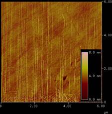
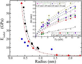
Figure caption. (a) AFM image
of horizontally aligned SWCNTs grown on quartz substrate; (b) Measured radial
modulus (Eradial) vs. SWCNT radius (black
squares) compares with data from nanoindentation experiment (blue dots) and modified MSM calculation data (red triangles, data
courtesy of Mr. Y.L. Liu). Inset: The measured radial deformation (Dh)
vs. applied normal force (Fz) as well as the fitting
to the experimental data by using the power function relation Δh∝Fz2/3 for SWCNTs with radius from 1.91 to 0.42 nm. For details, please see Yang et
al., APL 98, 041901, 2011.
·
Growth
Mechanism and optical properties of Ruthenium Dioxide and Nickel Oxide Nanostructures
(1) RuO2: Low-dimensional RuO2 nanostructures hold a promising future in nanoelectronics application due to their low resistivity and excellent thermal and chemical stabilities over a wide temperature range. The understanding of the growth mechanism of the RuO2 nanostructures is essential for controlling their growth and developing novel devices. We have studied the growth mechanism by combing experiment and electronic structure calculation. The experiment reveals that the O2 flow rate, concentration and pressure play significant roles in the formation of RuO2 nanostructures, as show in the Figure. Our calculation confirms that RuO2 has higher energy compared to RuO3 and RuO4. The less stable RuO3 (as compared to RuO4) is more suitable for nanorod growth and a rich O2 environment at the RuO2 source is a preferable condition to grow RuO2 nanorods.
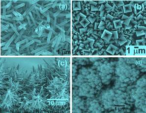
Figure
caption. RuO2 nanostructures synthesized at various conditions. (a)
Polygonal prisms with uniform width formed at low O2 flow rate, (b) top-view
of nanorods with square-shaped hollow tips at high O2 flow rate, (c)
hierarchical pine tree-liked structure formed at high
pressure, and (d) flower-liked nanostructures formed at low O2 concentration. For details, please see Neupane et al. Journal of Materials Sciences 46, 4803 (2011).
(2)
NiO: NiO
nanowalls have demonstrated their potential use as field emitter, electrodes
for high performance Lithium ion battery and electrochemical
supercapacitor.Vertically aligned and well interconnected NiO nanowalls with
thin nanodiscs of cubic NiO as the in
situ formed building blocks were fabricated via a template-free approach.
Surface morphology analysis confirmed the formation of 15 nm thick and 1-1.5 μm wide nanowalls which
have the crystal structure of cubic NiO with their growth plane along the [111]
direction. An optical band gap of about 3.8 eV for the NiO nanowalls was
obtained from the optical absorption measurement. NiO nanowalls exhibited a
broad UV emission band centered at around 390 nm.
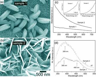
Figure caption. (A) SEM image
of a large area of the NiO nanowalls synthesized at 100 oC for 24 h (sample 1);
(B) SEM image of the NiO nanowalls synthesized at 200 oC for 24 h (sample 2);
(c) UV-vis absorption spectra for NiO nanowalls for sample 1 and sample 2, respectively.
Insets show the plot of (ahg)2 vs. hg for sample 1
and sample 2, respectively; and (d) Photoluminescence emission spectra for NiO nanowalls for sample 1 and
sample 2, respectively. For details,
please refer to Kumari et al., “Vertically Aligned and Interconnected Nickel
Oxide Nanowalls Fabricated by Hydrothermal Route”, Crystal Research and
Technology 44, 495 (2009).
·
Structure of
Flattened Carbon Nanotubes
Carbon nanotubes (CNTs) behavior either as semiconductor or metal depending on the arrangement of carbon atoms in their cylindrical graphitic layers. However, CNTs are not always in cylindrical shape, they could be partially or fully collapsed to form flattened CNTs (F-CNTs). The F-CNTs have substantially different electrical properties from their cylindrical counterparts. Therefore, a detailed study on the structure of the F-CNTs is essential to the understanding of the electrical property and the application of CNTs. In this research, the structure of the F-CNTs has been investigated by transmission electron microscopy (TEM). Two types of flattenings of CNTs in our experiment have been observed. The first type of flattening is parallel to and symmetric about the long axis of the CNT. The second type of flattening is a spiraling of fully flattened CNT around the long axis of the CNT. The flattening and the spiraling are ascribed to axial compression and torsion on the CNTs.
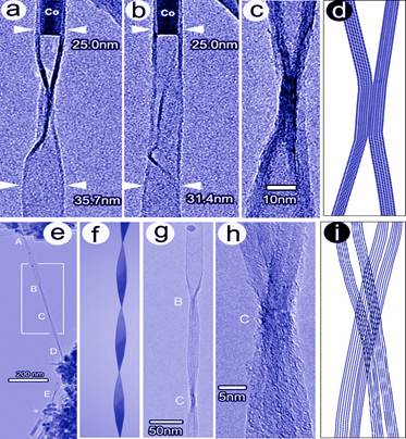
Figure caption. TEM images
of a F-CNT capped with Co catalyst particle before (a)
and after (b) rotation of 35°. A CNT with parallel flattening
(c) and its model (d). A long spiraling of a fully flattened CNT (e),
its model (f), its close-up (g), the high magnification of a node C (h), and
the model of the node C (i).
For details, please see Li et al., “Structure of
flattened carbon nanotubes”, Carbon 45, 2938 (2007).
·
Electrical properties of
carbon nanotube junctions
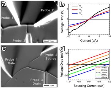
The
electrical properties of the carbon nanotube junctions were investigated using
4-probe scanning tunnelling microscope (STM). The transport property
measurement was carried out on three terminal junctions such as T-junction (Figure
a) and Y-junction (Figure c). In contrast to the reported three
terminal nanotube junctions where a rectification-like asymmetric I –V behaviour has been reported, the
T– or Y– junctions here display symmetric I –V curves. For the T–junction, the I –V curves measured with two probes across the junction are
nonlinear at a high source current range (Figure b); however, they are
linear at a low source current range, similar to that of the Y-junction (Figure
d). Both types of junctions do not show a gate effect when a bias voltage
is applied to one of the branches while the transport is measured between the
other two branches. When the silicon substrate was used as the back gate, the
gate effect of the junction nanotubes was not observed either. The lack of
rectifying behaviour and gating effect is consistent with the metallic
conduction state of the junctions. For details, please refer to Kim et al, Nanotechnology 19, 485201 (2008).
·
Growth mechanism of carbon
nanotube junctions
The
research emphasis is on studying, identifying and understanding fundamental
mechanisms of synthesis of new functional materials - Y-shaped carbon nanotube
junctions (Y-junctions). In this project, thiophene (C4H4S) has been used as
carbon source to grow nanotubes on Co catalyst nanoparticles, and the influence
of the concentration of C4H4S vapor on the structure of
the nanotubes has been investigated. It is found that nanotube junctions will
grow when the C4H4S concentration is in the range of
0.76-1.5%. Otherwise, carbon fibers will form at high C4H4S
concentration and Co9S8 nanowire-filled nanotube will
form at low concentration.
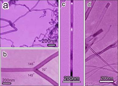
Figure caption.
Transmission electron microscopy images of (a) carbon fibers, (b) branched
nanotube, (c) Co9S8 nanowire-filled nanotube, and (d)
hollow nanotubes grown at various thiophene (C4H4S)
vapor concentrations 3.0, 1.5, 0.51, and 0.37 vol.%,
respectively. For details, please
refer to Li et al, J. Phys. Chem. B 110(47), 23694 (2006); Du et al., J. Phys. Chem. C, 2007, 111, (39), pp 14293–14298; Du et al, J. Phys. Chem. C, 2008, 112, (6), pp 1890–1895